
Semiconductor Industry: Growth Frontiers, Strategic Shifts, and the Rise of Emerging Economies
The semiconductor industry stands at the threshold of unprecedented transformation, underpinned by artificial intelligence (AI), advanced packaging, and strategic realignments in global supply chains. This article presents a comprehensive analysis of the semiconductor sector’s outlook from 2025 to 2035, highlighting key market dynamics, technological evolution, and the rise of new players. In parallel, it explores how emerging economies—specifically Bangladesh—are positioning themselves within this high-value global ecosystem through design, OSAT, and international collaboration. This article combines macroeconomic forecasts with structural, technological, and policy-driven developments shaping the next decade.
The Global Semiconductor Landscape in 2025
Market Overview
The semiconductor industry is projected to grow from US$627 billion in 2024 to US$697 billion in 2025—an 11.2% YoY increase—primarily driven by demand for AI accelerators, data center infrastructure, and advanced computing workloads. Projections from the World Semiconductor Trade Statistics (WSTS) anticipate further growth of 8.5% in 2026, reaching approximately US$760 billion.
Key Segment Drivers
- Logic (AI, GPU, ASIC): Expected to expand ~24% in 2025 (~US$267B), fueled by investments in AI inference and training systems.
- Memory (DRAM, NAND, HBM): Forecast to grow 11–13%, with high-bandwidth memory (HBM) rising by ~70% amid AI-centric workloads.
- Analog and Sensors: Moderate growth (~4–7% CAGR) from automotive and industrial IoT.
- Weak Segments: Discrete semiconductors, optoelectronics, and microcontrollers are flat or contracting due to demand correction and overcapacity.
Regional Dynamics
- Americas: Leading growth (~18%), spurred by CHIPS Act funding and fab expansion.
- Asia-Pacific: Sustained growth (9–10%), with major capacity in Taiwan, South Korea, and China (via Big Fund III, US$47.5B).
- Europe & Japan: Stable 3–4% growth, with the EU targeting 20% global share by 2030 via the EU Chips Act.
Technology and Manufacturing Trends
- Advanced Nodes: Mass production of 3 nm; 2 nm projected by 2025–2026; R&D on sub-1 nm devices is accelerating.
- Packaging Innovations: Heterogeneous integration (chiplets, SiPs), and advanced 2.5D/3D packaging (e.g., CoWoS, Foveros) are central to AI performance scaling.
- Sustainability: Chiplet-based designs may reduce embodied carbon by up to 70%, driving greener scaling.
Decadal Forecast (2025–2035): From $700B to $2 Trillion+

The consensus projects the industry crossing the US$1 trillion mark by 2030, with exponential growth in:
- AI/ML acceleration hardware
- Electrification of vehicles
- 5G/6G and edge computing
- Semiconductor industrial policy globally
Emerging Vertical Markets
- Automotive: EV and ADAS semiconductors growing ~30% CAGR; expected to exceed US$100B by 2025.
- AI/Cloud Infrastructure: Generative AI chip market projected to reach US$150B in 2025. AMD estimates a US$500B TAM by 2028.
- IoT & Telecom: Telecom semiconductors forecast to reach ~US$79B by 2032 (~25% CAGR in cellular IoT chips).
Policy and Investment Initiatives
- U.S. CHIPS Act: Allocating US$39B+ to regain leadership in logic manufacturing.
- EU Chips Act: €43B investment targeting strategic autonomy.
- India Semiconductor Mission: Targeting US$100–110B industry by 2030.
- China’s Big Fund III: US$47.5B fund driving indigenous AI chip development.
Strategic Industry Leaders and Technological Influence:

Global Champions:
- NVIDIA: Market cap of US$3.5–4T; controls ~80% of AI GPU market.
- TSMC: Largest foundry (55% market share); drives 3nm/2nm production.
- Samsung: Memory leader; expanding logic foundry share (~40% of DRAM market).
- AMD: Competitive in AI (MI350/MI400 series); MI400 architecture to debut in 2026.
- Intel: Pivoting to system-level AI, faces delays in 18A node execution.
- ASML: Exclusive supplier of EUV lithography; essential for sub-5nm transitions.
Emerging Players:
- Cerebras Systems: Introduced WSE-3, world’s largest AI training chip.
- MetaX (China): A challenger in the domestic AI chip market.
- Amazon, Google, Microsoft: Expanding availability of cloud-native accelerators.
Materials and Structure of Semiconductors
Material Foundations
Semiconductors are primarily based on elemental or compound materials that exhibit controllable electrical conductivity. The most widely used base material is pure silicon (Si), owing to its natural abundance and excellent semiconductor properties. Other notable materials include:
- Germanium (Ge) – An early semiconductor material, now mainly used in specialized applications.
- Gallium Arsenide (GaAs) – Preferred for high-frequency radio frequency (RF) and 5G applications.
- Silicon Carbide (SiC) and Gallium Nitride (GaN) – Employed in power electronics such as electric vehicles (EVs), renewable energy, and high-efficiency converters.
Intrinsic vs. Doped Semiconductors
- Intrinsic Semiconductors refer to the pure form of materials, such as undoped silicon.
- Extrinsic Semiconductors are doped with specific impurities to enhance conductivity: N-type: Doped with elements like phosphorus or arsenic to increase electron carriers. P-type: Doped with boron or gallium to create hole carriers.
Semiconductor Structural Framework
Wafer and Layered Architecture
Modern semiconductor devices are constructed on silicon wafers, typically 300 mm in diameter, using a sophisticated layered architecture:
- Oxide Layer: An insulating layer (usually SiO₂) formed by thermal oxidation.
- Polysilicon Layer: Utilized in gate formation for transistors.
- Metallization Layers: Copper or aluminum layers that provide electrical interconnects.
- Transistor Layer: Primarily composed of CMOS (Complementary Metal-Oxide-Semiconductor) structures combining NMOS and PMOS transistors.
Fabrication Process

Types of Semiconductor Implementations
- Digital: CPUs, GPUs, ASICs – rely on binary logic.
- Analog: RF modules, amplifiers, sensors.
- Discrete vs. Integrated Circuits: Discrete: Single-function components (e.g., transistors, diodes). Integrated: Multi-functional, large-scale integration (e.g., SoCs).

Advanced Packaging and Integration
- 2.5D/3D ICs: Vertical and planar integration to enhance performance and reduce latency.
- Chiplets: Modular functional blocks interconnected via high-speed links (e.g., AMD EPYC).
- Fan-Out Wafer-Level Packaging (FOWLP): Enhances I/O density and form factor.
- CoWoS/EMIB: Cutting-edge interconnect technologies developed by TSMC and Intel.
Emerging Technologies:

Semiconductor Development Lifecycle
Semiconductors are the foundational technology driving the digital age. Whether powering mobile devices, enabling AI computation, or supporting infrastructure systems, modern chips require a highly coordinated development lifecycle. This lifecycle integrates multiple disciplines—including design, fabrication, packaging, and validation—into a seamless yet complex pipeline. Understanding the full scope of this process is critical for advancing innovation, improving efficiency, and making strategic decisions in technology policy and investment.
Phases:
- Concept & Feasibility
- Architecture & Planning
- RTL Design & Verification
- Physical Design (Back-End)
- Tape-Out & Fabrication
- Packaging & Assembly
- Testing & Validation
- Production & Yield Optimization

Each phase encompasses specialized tasks and outputs, involving cross-functional teams and Electronic Design Automation (EDA) tools.

Strategic (Core) Phases of Semiconductor Development
1. Planning & Design: The Innovation Engine
This phase defines what the semiconductor will do and how it will function. It is R&D intensive and demands skilled human capital and advanced Electronic Design Automation (EDA) tools.
Key Activities: – Architecture design, RTL development, verification, tape-out – Tools: Synopsys, Cadence, Siemens EDA – IP Providers: Arm, Imagination – Bangladesh Focus: Invest in semiconductor curriculum at universities, enable design incubators, partner with global EDA vendors for tool access
2. Fabrication: Capital-Intensive Manufacturing
This phase transforms designs into physical chips on silicon wafers using nanometer precision. It is highly capital intensive and centralized in a few global foundries.
Key Activities: – Wafer processing, yield optimization, probe testing – Foundries: TSMC, Samsung, Intel – Timeline: 8–12+ weeks – Bangladesh Focus: Explore joint ventures with regional foundries, develop Special Economic Zones (SEZs) for semiconductor manufacturing, ensure critical raw material access
3. Packaging & Testing: Market Readiness
After fabrication, chips are diced, packaged, tested, and classified. Advanced packaging is vital for applications from smartphones to data centers.
Key Activities: – Packaging (e.g., BGA, FOWLP, chiplets), assembly, functional and thermal testing – Vendors: ASE Group, Amkor, OSAT providers – Bangladesh Focus: Develop testing and packaging hubs in partnership with global players, leverage existing electronics manufacturing base, integrate with export strategy.

Summary Table: Semiconductor Value Chain

Semiconductor Job Market Outlook – Global & Bangladesh
Global Landscape
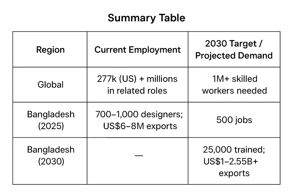
- Surging Demand: AI, electrification, and data centers are fueling semiconductor growth, with Deloitte estimating a need for 1+ million skilled workers by 2030.
- Talent Gap: In the U.S., CHIPS Act projects 160,000 new roles, but with only ~2,500 new entrants annually, a shortfall of 146,000 workers is expected by 2029.
- Current Workforce: U.S. employs ~277,000 directly in semiconductors; Germany’s “Silicon Saxony” employs ~70,000.
- Emerging Solutions: Fast-track upskilling programs and industry partnerships are being used to close the skills gap.
Bangladesh Landscape
- Current Status: Semiconductor exports are US$6–8M annually, primarily from design firms (Ulkasemi, Neural Semiconductor, Prime Silicon) employing 700–1,000 designers. Educational programs exist, but lab and cleanroom facilities remain limited.
- Growth Targets:
- Ulkasemi: 500 jobs by 2025, 5,000 by 2030.
- Growth Targets:Ulkasemi: 500 jobs by 2025, 5,000 by 2030. Train 25,000 engineers by 2030 for US$1B exports. Policy vision: Up to US$10B industry by 2040, 100000 professionals, potentially 4–5% global market share.
- Human Capital: ~25,000 EEE/CSE graduates annually; targeted specialization could meet industry needs. Requires curriculum reform, hands-on labs, and industry-academic collaboration.
Strategic Takeaways
- Global: Severe skills shortage presents opportunities for countries with rapid talent development capacity.
- Bangladesh: Positioned to emerge as a competitive design, testing, and packaging hub. Achieving training targets could generate billions in export revenue. Success depends on education reform, infrastructure investment, public–private partnerships, and global linkages.
Bangladesh in the Global Semiconductor Ecosystem
National Strategy and Sectoral Entry Points
Bangladesh is adopting a focused approach to enter non-fab segments such as chip design, OSAT (Outsourced Semiconductor Assembly and Testing), and packaging. As of 2025, exports stood at US$6 million, with a national roadmap targeting US$1 billion by 2030.
Strategic Priorities:
- Design and Verification: Companies like Ulkasemi, a TSMC DCA member, provide ASIC, IP, and physical design services.
- OSAT Hubs: Proposed in Hi-Tech Parks (e.g., Kaliakoir), supported by PPPs and regional collaborations (notably with Malaysia).
- Talent Pipeline: Engineering university lab, BASICS Program, and government initiatives aim to certify 25,000 VLSI engineers by 2030.
- International Collaboration: Diaspora-led mentorships, trilateral partnerships (e.g., Korea–Malaysia–Bangladesh), and JV formation with global firms.
Development Phases for Semiconductor Services

Conclusion and Outlook
The semiconductor industry is not merely a technology domain, it is increasingly at the core of economic resilience, geopolitical sovereignty, and environmental sustainability.
Global Outlook:
- 2025–2026: Surging demand from AI, packaging innovations, and logic semiconductors.
- 2025–2030: Growth driven by EVs, telecom modernization, and IoT proliferation.
- 2030–2035: A potential US$2–2.8T market, underpinned by chiplet architectures, sub-nanometer fabrication, and carbon-conscious innovation.
Bangladesh’s Role: By targeting OSAT and chip design, supported by skilled labor, strategic partnerships, and proactive policy frameworks, Bangladesh is poised to establish itself as a credible emerging hub in the global semiconductor value chain by 2030.
Note: The coming decade in semiconductors will be defined not just by advancements in nanometer scaling or processing power, but by broader strategic imperatives: national resilience, environmental sustainability, and equitable global access. Nations such as Bangladesh are no longer passive observers of this transformation. They are emerging as active participants, positioning themselves as co-architects in shaping the next wave of digital innovation and industrial progress.
Engr. Johnny Shahinur Alam
Technologist and ICT & Digital Transformation Specialist